CORIAL's Top 5 Blog Posts of 2021
As a Plasma-Therm company and leader in the plasma-processing and advanced-packaging industry, our finger is on the pulse of the semiconductor and nanotechnology markets. Over the past year, we’ve shared educational and informative information regarding plasma-etching, deposition, product highlights, and other relevant tech news and updates....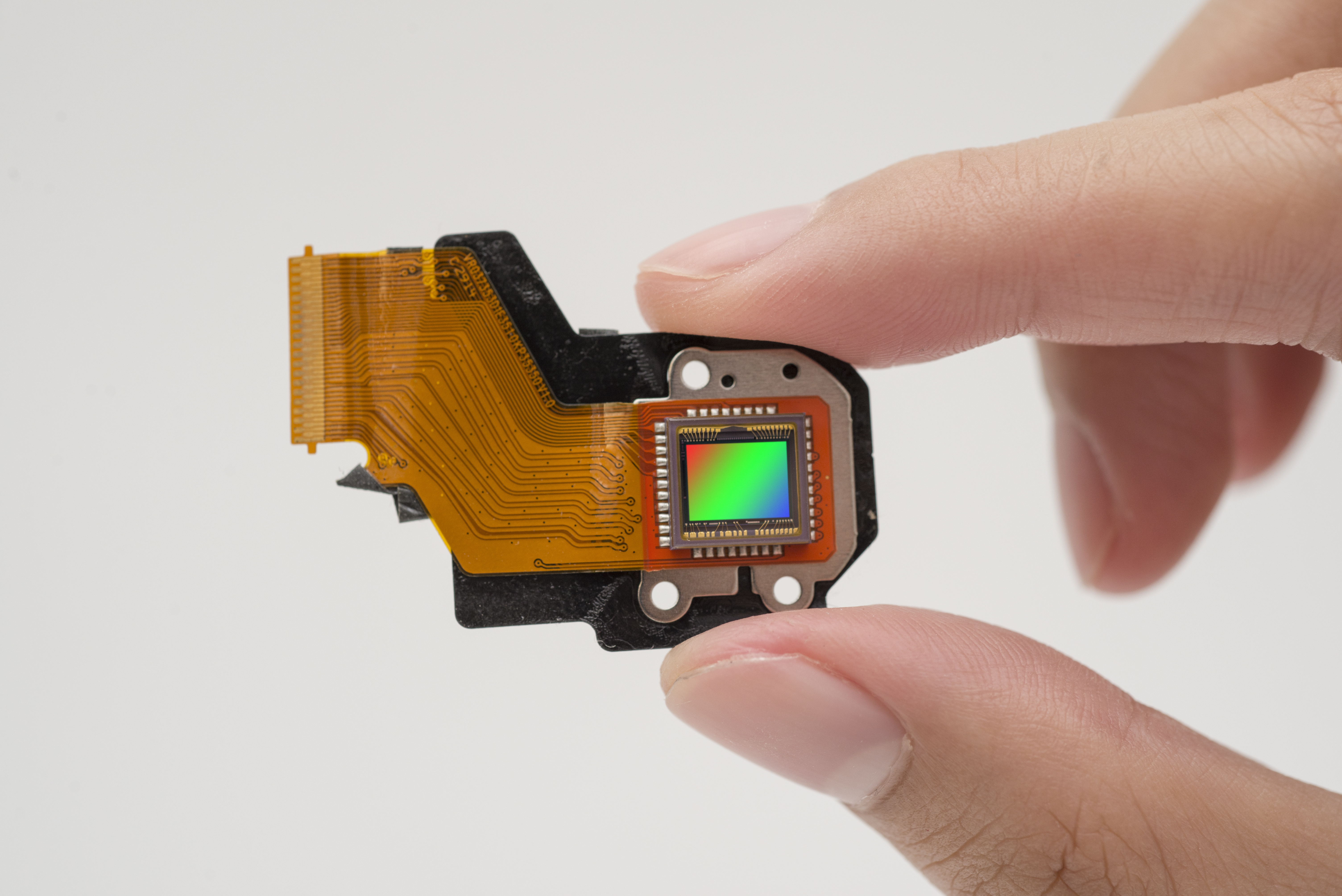
3 Specialized Etch Processes for Photonics Fabrication
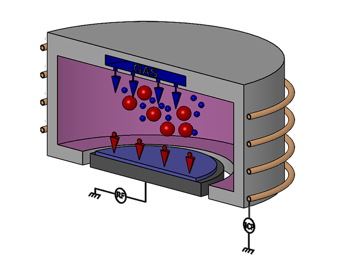
There are typical etch processes that are used in nearly every process flow, but there are also specialized etch processes that are specific to unique aspects of the application. Photonics manufacturing is no exception. Whether fabricating image sensors or photonic circuits, dry etch processes will be key to creating features with excellent optical properties....
How to Minimize Downtime for Etch and Deposition Equipment
Semiconductor plasma etch and deposition equipment has drastically different usage profiles when used in industry as compared to its use in research and academia. While the physics governs both applications, their end uses are different, and thus require different considerations for optimization....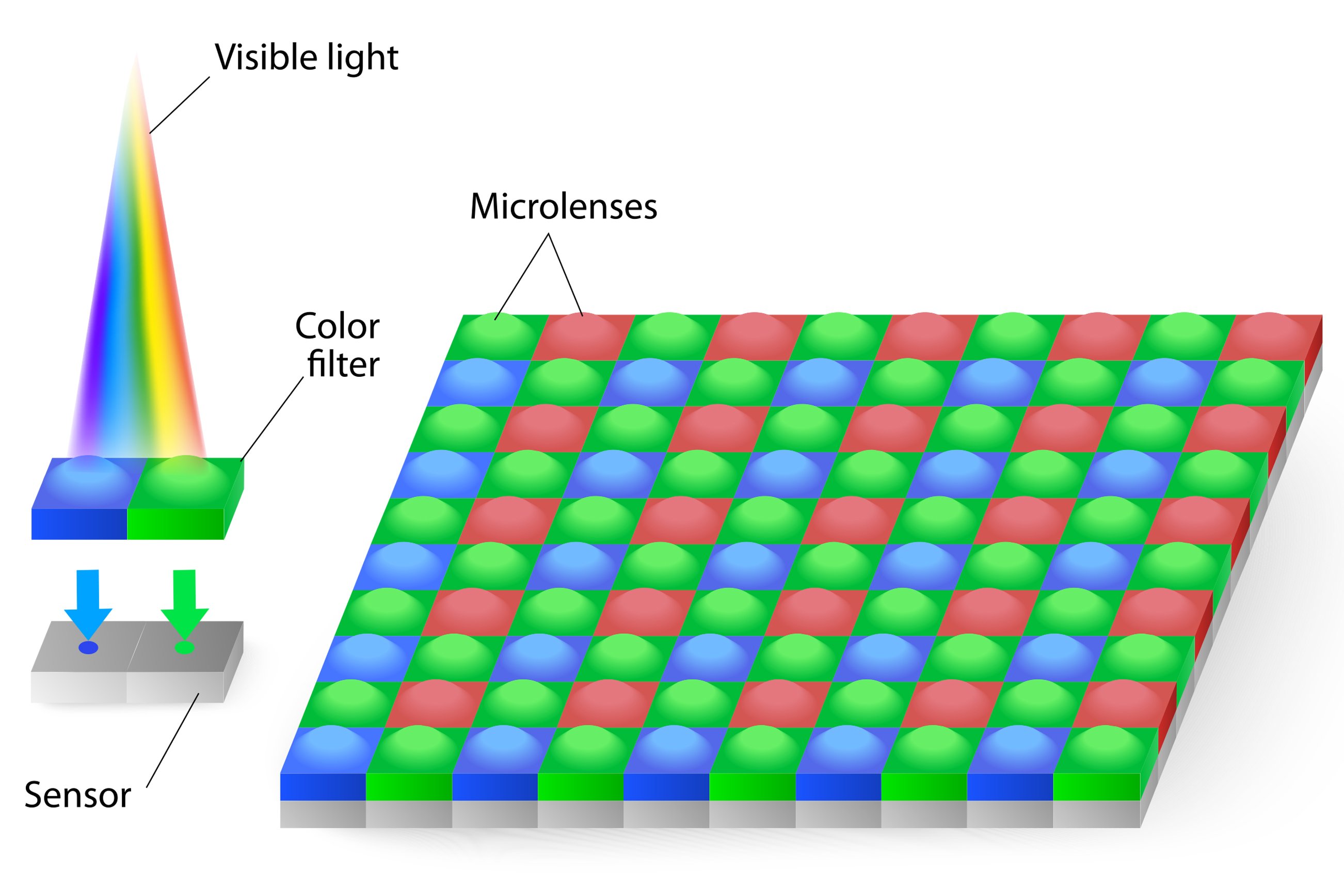
Bringing Micro-lenses Into Focus
It is not surprising that the scaling techniques used to enable Moore’s Law over the last several decades are being applied to similarly scale down the structures using macro-optics. As feature sizes of transistors have shrunk so that millions to billions of transistors fit on a chip, optical components have also been reduced in size. Many of these efforts are leading the way for advances in photonics. For example, chip-to-chip connections with relatively large fiber optics have evolved such that micron-sized chip-scale waveguides for making photonic based interconnects are now a possibility. Similarly, micro-lenses are opening up new applications that were once the domain of macro-lenses. This article introduces micro-lenses and how they are made using semiconductor processing techniques....
Etching of Difficult Metals
Over time three primary approaches have been developed to pattern metals: Wet etching, a physical deposition approach known as “lift-off,” and plasma etching. Wet etching, while having relatively low associated equipment costs, are limited by the isotropic nature of the etch mechanism. In this subtractive method, the isotopic etching behavior is only useful for features with non-critical dimensions (e.g. >~5 μm). There is no doubt that wet etching has applicability to larger features where the amount of undercut is small in relation to the feature size. Although wet etching processes are typically highly selective, the extremely reactive reagents often needed to etch metal may damage other exposed materials....