Production-proven equipment and processes for the optoelectronics industry

Optoelectronics market overview

Optoelectronics is the branch of electronics that combines optics and electronics. Devices can be divided into two categories – light-sensitive devices and light-generating devices.

Optoelectronic devices can be used in two major end-markets – solid state lighting and photovoltaics.

Some of the common light-sensitive devices used in electronic circuits are photodiodes, phototransistors, light sensitive resistors, photovoltaic cells, and more. Light-generating optoelectronic devices include Laser Diode, High Brightness Light Emitting Diode (HB-LED), Organic LED (OLED),…etc. Some devices combine both the principles of sensitive and light generating devices like Light Dependent Resistors (LDR), Liquid Crystal Displays (LCD), optoisolators, optoreflectors and more.

CORIAL solutions

CORIAL has been providing equipment and processes for the optoelectronics industry for more than 12 years.

CORIAL etch and deposition technologies are designed to handle the wide range of materials required for optoelectronic devices fabrication, including sapphire, GaN, Si3N4 and SiO2.

AdvantagesCORIAL Advantages

R

Unmatched process flexibility for optoelectronics manufacturing

R

Expertise for sapphire patterning on 4" and 6" wafers

R

Low cost of ownership

processEtch processes

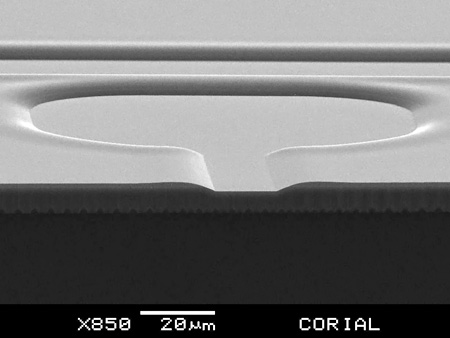
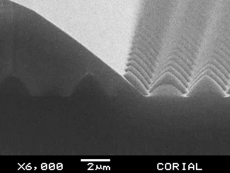
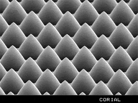
We have broad experience processing a wide range of materials with precise control of the etch profile, fast etch rates, and excellent etch uniformity.

GaN etch for Mesa structuring (LED manufacturing)

  • Etch rate 650 nm/min
  • Etch depth 1.5 µm
  • Uniformity ± 3%

GaN etch for device isolation

  • Etch depth 7 µm
  • Etch rate 1200 nm/min
  • Uniformity ±2 %

Sapphire etch for PSS application

  • Etch rate 100 nm/min
  • Edge exclusion 2 mm
  • Uniformity ±2 %

processDeposition processes

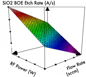
The optoelectronics industry necessitates the use of a wide range of dielectric films.

Depositing thin SiO2 and Si3N4 films used as passivation or current blocking layers, CORIAL delivers processes that ensure tight control of film stress (tensile to compressive), and fast deposition rates without any compromise in deposition uniformity, or film quality (low BOE etch rates for SiO2, low KOH and TMAH etch rates for Si3N4).

Fast and high-temperature SiO2 deposition (hard mask)

  • 1 µm thick deposited at 280°C
  • Deposition rate 110 nm/min
  • Refactive index 1.68

Si3N4 deposition at low RF (photodiodes)

  • RF power 20 W
  • Deposition rate 5 nm/min
  • Refractive index 1.81

Low-temperature SiC film deposition (OLED)

  • Deposition rate 30 nm/min
  • Deposition at 80°C
  • Stress 10 ± 50 MPa

processProducts

Corial 210IL process

Corial-210IL-zoom
  • ICP-RIE etch system with load-lock
  • Fast etch rates for III-VI compounds
  • Cluster configuration for integration on the Corial PS200

Corial D250 process

Corial-D250-Zoom
  • PECVD system with in-situ plasma cleaning
  • Low temperature PECVD on organics
  • High temperature SiO2, Si3N4, SiOCH, SiOF, SiC and aSi-H films deposition

Corial D250L process

Corial D250L
  • Same capabilities as Corial D250, plus vacuum load-lock for higher throughput

Corial 360RL process

Corial-360RL-Zoom
  • Large area RIE etch system
  • Manual loading for batch up to 7 x 100 mm wafers
  • GaAs, GaP, InP, GaN and AlGaN etch

Corial 360IL process

Corial-360IL-zoom
  • ICP-RIE etch system for 24/7 production environment
  • Load-lock for batch up to 7 x 100mm wafers
  • Fast etching rates for sapphire, III-V compounds

Corial D350 process

Corial-D350-Zoom
  • PECVD deposition system for 24/7 production environment
  • Manual loading for up to 300 mm wafers
  • High quality SiO2, Si3N4, SiOCH, SiOF, SiC and aSi-H films deposition

Corial D350L process

Corial-D350L-Zoom
  • Same capabilities as Corial D350, plus vacuum load-lock for higher throughput

Corial D500 process

Corial-D500-Zoom
  • Very large area PECVD deposition system
  • High throughput: 104x2’’ ; 25x4’’ ; 9 x 6’’ or plates up to 500 mm x 500 mm