Exceptional process flexibility, from high SiC etch rates to low damage film deposition

Power devices market overview

Demand for wide bandgap power semiconductor components is principally driven by growth of the hand-held devices market, where efficient power management is appreciated key requirement.

The exponential growth in the adoption of green energy sources for industrial and consumer markets (wind power, solar cells, electric vehicles, etc.) is another driver for wide bandgap semiconductors. These materials are a critical part of high current/high voltage devices.

CORIAL solutions

Silicon carbide (SiC) and gallium nitride (GaN) are materials of choice in the manufacture of power semiconductor devices.

CORIAL offers equipment that specifically target etch and deposition processes for compound semiconductor-based power devices.

AdvantagesCORIAL Advantages

R

Equipment is easily scalable from R&D to volume production

R

Retractable liner protects reactor, and collects etch by-products

R

One chamber for all wafer sizes

processEtch processes

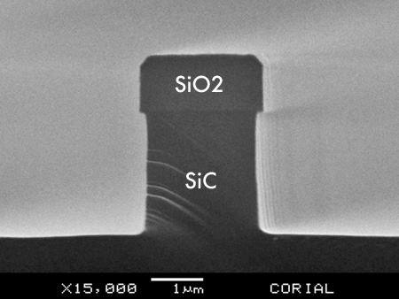
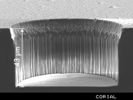
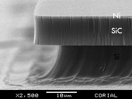
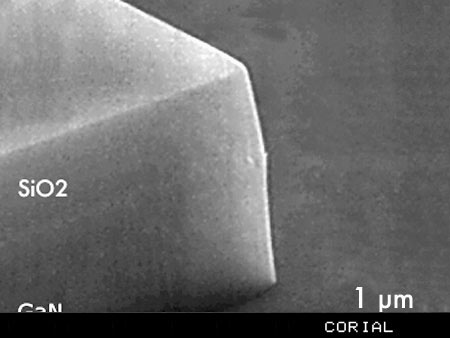
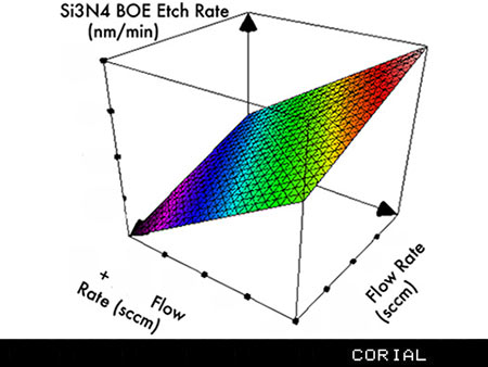
Power semiconductor device manufacturing requires a range of dry etch processes, including deep trench etch, smooth feature etch, and low damage etch.

SiC DRIE

  • Smooth sidewalls
  • Etch rate 0.7 µm/min
  • Selectivity vs mask > 2.5:1

SiC via etch

  • > 100 µm etch depth
  • Etch rate 1.4 µm/min
  • Selectivity vs. Ni mask > 15:1

SiC feature etch

  • Etch depth > 1 µm
  • Etch rate 0.8 µm/min
  • Roughness < 5 nm

GaN Feature etch

  • Anisotropic etch
  • Etch rate 200 nm/min
  • Low plasma damage

processDeposition processes

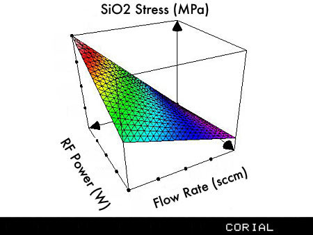
Typical plasma enhanced deposition applications for power device manufacturing include passivation, dielectrics, and masks. CORIAL’s PECVD tools are designed to ensure tight control of film stress, from tensile to compressive, and to produce high deposition rates films without any compromise in uniformity or film quality. CORIAL also offers low temperature and low damages PECVD processes for nitride and oxide films.

High-quality Si3N4 film deposition

  • Deposition rate 110 nm/min
  • Refractive index 2.045
  • Stress -100 ± 50 MPa

SiO2 layer with tunable stress for passivation

  • Deposition rate 350 nm/min
  • BOE etch rate <240 nm/min
  • Stress 10 ± 50 MPa

Thick SiO2 film deposition for hard mask

  • 100 µm thick layers
  • Deposition rate 550 nm/min
  • No manual cleaning required

processProducts

Corial 210IL process

Corial-210IL-zoom
  • High density ICP source for rapid etching of hard materials
  • Excellent process repeatability
  •  Excellent particle control (liner)

Corial D250 process

Corial-D250-Zoom
  • PECVD system with in-situ plasma cleaning for high uptime
  • High and low temperature PECVD
  • SiO2, Si3N4, SiOCH, and SiC film deposition

Corial D250L process

Corial-D250L-Zoom
  • Same capabilities as Corial D250, plus vacuum load-lock for higher throughput

Corial 360IL process

Corial-360IL-zoom
  • ICP-RIE etch system for 24/7 production environment
  • Batch sizes up to 7 x 100 mm wafers
  • Fast GaN etch rates

Corial D350 process

Corial-D350-Zoom
  • PECVD deposition system for 24/7 production environment
  • Manual loading for up to 300 mm wafers
  • High quality SiO2, Si3N4 films deposition

Corial D350L process

Corial-D350L-Zoom
  • Same capabilities as Corial D350, plus vacuum load-lock for higher throughput

Corial D500 process

Corial-D500-Zoom
  • Very large area PECVD deposition system
  • High throughput: 104x2’’ ; 25x4’’ ; 9 x 6’’ or plates up to 500 mm x 500 mm