.jpg)
The ability to pattern silicon has been the foundation of modern electronics. Depending on the specific application there are multiple methods to consider. Here we will focus on dry etching and constrain the discussion to well-known methods that can deliver anisotropic (as opposed to isotropic) features.
From a high-level perspective, we can divide silicon applications into groups such as electronic (e.g. CMOS), photonic (e.g. optics, waveguides, and detectors), and microelectromechanical systems (e.g. MEMS and MOEMS). However, perhaps a better (but not perfect) dividing characteristic is the feature etch depth, and it this where we typically define the boundary between etching technologies. In this discussion, we will arbitrarily refer to deep silicon structures when the etching depth exceeds 3 um (far beyond that used for mainstream silicon-based device fabrication). Using this feature depth as a guide, we will discuss the two common etching methods for deep reactive ion etching of silicon (DRIE).
DRIE has traditionally been divided into two process approaches. The first technology has been referred to by several names which, unfortunately, can lead to confusion. The most common is DRIE but since this acronym implies an application for deep silicon structures, it does not distinguish between process approaches. For this reason, it is useful to specifically use the term “Bosch Process” (named after the company holding the original patent) or TDM (time division multiplexed). For simplicity, we will use the Bosch nomenclature despite some of the controversy surrounding this name and patent. The second approach we will call non-Bosch or single-step DRIE.
Non-Bosch Processes
The goal of DRIE is to etch deep structures while maintaining relevant critical dimensions. To achieve the requisite anisotropic profile and take advantage of the directionality offered by ion assisted processes, some sort of sidewall passivation is needed. The sidewall passivation acts to protect the sidewall by inhibiting lateral or isotropic etching. Several process chemistries were developed to accomplish that passivation with the most well-known using C4F8/SF6 and the other using SF6/O2.
The combination of C4F8/SF6 provides both the fluorine radicals (F*) needed as a reactant to etch silicon and the fluorocarbon fragments that can easily generate surface polymers. The fluorocarbons provide a conformal layer of polymer that remains after ions arriving normal to the surface preferentially remove the polymer on the “floor” or bottom of the feature being etched. Without the protective polymer, the reactive F radicals would etch in equally in all directions resulting in an isotropic profile. With the right mix of C4F8, SF6, pressure, and ion flux conditions, the etching profile can be confined with vertical sidewalls. The sidewall polymer requires removal post-processing.
Another non-Bosch approach is to use O2/SF6 chemistry at low temperatures. Although this process is called a cryo process, the -110C temperature is much higher than that of liquid nitrogen (-196C). Here the mechanism is similar to that of C4F8/SF6. However, in this case, low-temperature help with the formation of the sidewall passivation with a SiOF species serves to limit lateral etching. The SiOF at the bottom of the feature is again removed by the ions normal to the surface. Once the wafer returns to room temperature the SiOF desorbs.
Bosch Process
This process uses the same gases, C4F8 and SF6, as the non-Bosch process described earlier. However, in this case, the gases are separated in time. During one cycle the Si is etched using the F radicals from SF6 (without C4F8 present), and during another process step the characteristic C4F8 polymer is deposited without the SF6 present. Usually, the polymer at the bottom of the feature is removed with an additional step using the directional ions between the SF6 etch step and the C4F8 passivation step. These three steps constitute a cycle that is repeated until the appropriate etch depth is achieved. Although it would seem that Si etch rates would be slow since etching only occurs during the SF6 step, the contrary is true: Vertical profiles with etch rates of >25 um/min for relatively low aspect ratio features can be achieved. It is equally impressive that features with aspect ratios of 100:1 can also be realized.
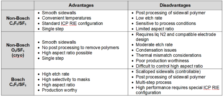
Comparison
Applications usually drive the choice of etch technology. While both non-Bosch and Bosch processes can achieve vertical profiles and very smooth walls, there are tradeoffs dependent on the application requirements. Tradeoffs include selectivity, throughput, sidewall morphology, feature profile, aspect ratios, and uniformity. The table below provides a guide to some of the advantages and disadvantages of the three techniques described in this article.
It should be noted that this is a brief introduction to these technologies and is not meant to cover the many detailed aspects of their performance or nuances.
To learn more, download our whitepaper comparing Plasma Etching technology: PE, RIE, and ICP-RIE.