Decades of experience providing solutions for IC delayering down to the 20 nm technology node

IC Failure Analysis market overview

The preparation of ICs for failure analysis, yield enhancement, or reverse engineering requires such techniques as sample deprocessing, and backside silicon access. These techniques can be performed with a plasma etch tool.

The quest for more powerful, smaller, and faster devices increases the need for more metal layers during the chip design and manufacturing processes.

Deprocessing is a challenging effort, as the device must retain electrical integrity, and its surface must remain planar for further investigation on the root causes of the failure.

CORIAL solutions

Semiconductor failure analysis requires techniques to remove the upper layers and intermetal dielectrics of diverse ICs, to expose a defect area that may be located beneath those layers.

From single or multilevel deprocessing without erosion of metallization layers for maintaining electrical investigation, to the most selective and damage free processes for metal etching, CORIAL RIE and ICP-RIE FA solutions enable sample preparation of dies, packaged dies and wafers up to 200 mm.

AdvantagesCORIAL Advantages

R

Delayering capabilities of dies, packaged dies and wafers up to 200 mm

R

CORIAL processes prevent sample over etch

R

Cost-effective systems

processEtch processes

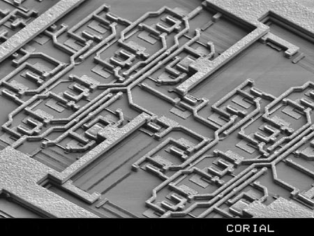
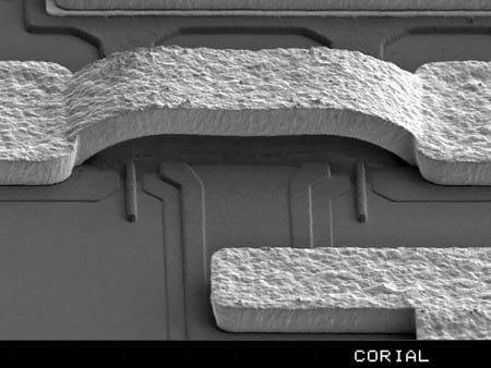
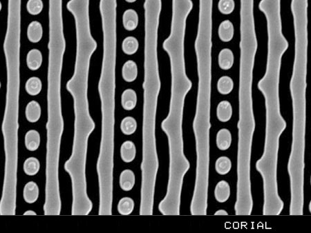
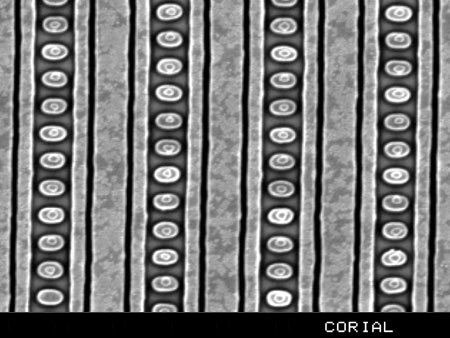
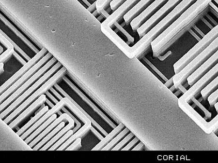
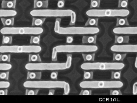
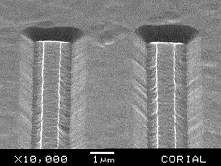
We have developed a variety of processes to enable individual or multi-layer removal of polymers, silicon compounds, ILD, low and ultra-low-K dielectrics, and metals.

Anisotropic Si3N4 layer etch on die

  • Si3N4 etching
  • Etch rate 500 nm/min
  • Selectivity vs. Al/Cu > 50:1

Isotropic Si3N4 removal on die for failure analysis

  • Si3N4 etching
  • Etch rate 700 nm/min
  • Selectivity vs. Al/Cu > 50:1

ICP etch process for die deprocessing in advanced technology nodes

  • Low-K dielectric etching
  • Etch rate 300 nm/min
  • Selectivity vs. Al/Cu > 50:1

ICP etch process for ultra-low-K delayering in 20 nm technology node

  • Ultra-Low-K dielectric etching
  • Etch rate 200 nm/min
  • Selectivity vs. Al/Cu > 50:1

Plasma technology for 4 metal layers exposure Al technology

  • 4 metal layers revealed
  • Al technology
  • No metal erosion

SiO2 revealed for failure analysis in 40 nm technology node

  • SiO2 etching
  • Etch rate 140 nm/min
  • Selectivity vs. metal > 50:1

ICP etch process for Si3N4 delayering in advanced technology node

  • Si3N4 etching
  • Etch rate 300 nm/min
  • Roughness < 5 nm

processProducts

Corial 200FA process

Corial 200FA
  • RIE etch system for deprocessing of dies and packaged dies
  • Confined high-density plasma that delivers fast and clean etching of SiO2, Si3N4, and polyimide layers
  • Automated EPD to prevent TiN or metals etch

Corial 200I process

Corial 200I
  • ICP-RIE etch system for deprocessing of wafers up to 200 mm
  • Si, SiO2, Si3N4, low-K/ultra-low-K, polyimide layers deprocessing and backside silicon thinning
  • Metal deprocessing capabilities (load-lock required)