Plasma etch
Forming nano-scale structures from a vast array of materials with RIE, ICP, and DRIE plasma etching technologies.

Fourth state of matter
Plasma is one of the four states of matter, along with solids, liquids, and gases. Plasma is an ionized gas consisting of equal numbers of positively-charged ions and negatively-charged free electrons. Thus, in plasma overall electrical neutrality is maintained.
Plasma is a common part of the world we live in. Along with nebula, interstellar space, and solar wind to mention a few, about 99% of the universe is made of naturally-occurring plasmas.
Plasmas are broadly used in technologies we interact with on a daily basis. Consider fluorescent lamps and neon signs – they are made of glass tubes filled with gas. When the lamp is turned on, the gas becomes ionized, electric current starts flowing through the tube, electric energy is dissipated, generating ions, electrons and excited molecules. This molecular excitation-relaxation process creates the characteristic plasma glow discharge inside the tube that illuminates the surrounding environment.
Plasma generation
The practical means to create plasma is to apply an electric field to a low-pressure gas.
Any free electron (created by a cosmic electron, for example) can be accelerated and gain enough energy to ionize a molecule by collision.
So, an electron/positive ion pair is created. The new free electron will continue the process and the plasma will be established by this chain reaction.
Plasma applications in the semiconductor industry
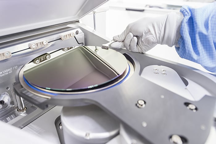
To manufacture integrated circuits, thin films of various material types are deposited, patterned, and etched. These process steps are repeated many times to build the integrated circuit layer upon layer.
“Dry” or plasma etching is one of the major processing steps in semiconductor manufacturing.
Once a material has been deposited onto the substrate (usually a silicon-based wafer), it is coated with photoresist or a hard mask. A photomask with the pattern corresponding to one layer of the IC is positioned above the wafer and exposed to UV light. The mask is opaque in some regions and transparent in others. In areas where the mask is transparent, the photoresist beneath the mask is exposed to light and becomes insoluble (this is applicable to so-called “negative” photoresist). Unexposed areas of the photoresist are removed by a chemical developer to reveal the underlying layer, which will be etched in the next processing step.
The etch process removes material in the exposed areas of the wafer surface, defining that pattern. After stripping the resist mask, another process step can be implemented.
Plasma etch processes can remove virtually all types of materials used in semiconductor industry: metals, dielectrics, semiconductors, and create a variety of structures from shallow recesses to 3D stacks.
Plasma etching principles
A gas containing a chemically reactive species (fluorine, chlorine…) is introduced and confined in an etch reactor at low pressure. Electromagnetic energy, typically in the MHz range of frequency, is then applied to one of the two electrodes of the reactor. Electrons, accelerated by the electric field, ionize the gas molecules. Excited molecules, radicals, ions, and electrons are thus formed upon electron impact.
The radicals chemically react with the exposed material on the wafer to form volatile or nonvolatile byproducts. At the same time, positively-charged ions bombard the wafer, which defines the required pattern.
Chemical adsorption
Chemical adsorption of atoms and radicals (neutral species) takes place on the surface to be etched. This mechanism is limited by the time required to form one monolayer of atoms on the etching surface. This time is inversely proportional to the pressure applied in the reactor.
Synthesis of volatile compounds
Volatile compounds are formed on the substrate surface. This mechanism may or may not be assisted by ion bombardment.
Desorption
Volatile compounds desorb from the substrate surface. Applying an RF bias to a wafer placed in the reactor attracts plasma ions and controls ion energy. Ion bombardment thus contributes to desorption of reaction byproducts and enables profile control.
Plasma etching advantages
In comparison to conventional wet etching techniques based on the use of liquid solutions, plasma (dry) etch processes offer several benefits.
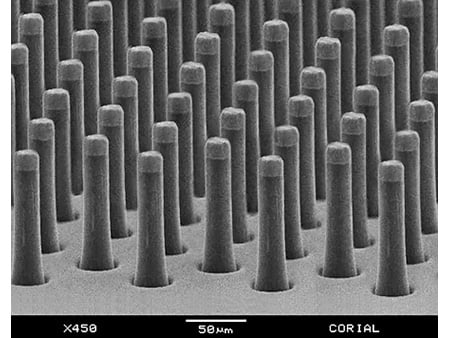
Tight control of structure profile
Nano-scale precision
Capability to etch hard materials
Cleaner and more environmentally-friendly process
Plasma etching technologies
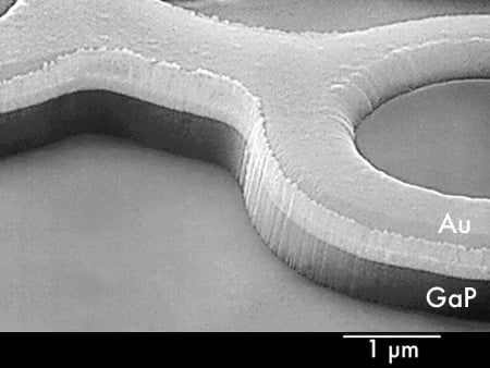
Reactive ion etching (RIE)
RIE technology is capable of etching a wide range of materials. Despite its various advantages, RIE applicability can be limited due to relatively low etching rates, depending on the material to be etched. Sputter-etching processes are also available with RIE.
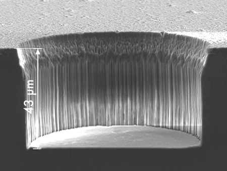
Inductively Coupled Plasma (ICP – RIE)
ICP-RIE is used to rapidly etch a wide range of materials, including semiconductors, dielectrics, metals, and polymers. The available processes span from low damage etch processes to the etching of hard materials.
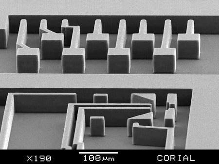
Deep Reactive Ion Etching (DRIE)
Deep etching of silicon and hard materials can be used to create micro-structures with high depth and high aspect ratios.
