There are typical etch processes that are used in nearly every process flow, but there are also specialized etch processes that are specific to unique aspects of the application. Photonics manufacturing is no exception. Whether fabricating image sensors or photonic circuits, dry etch processes will be key to creating features with excellent optical properties.
Etching Microlens for Image Sensors
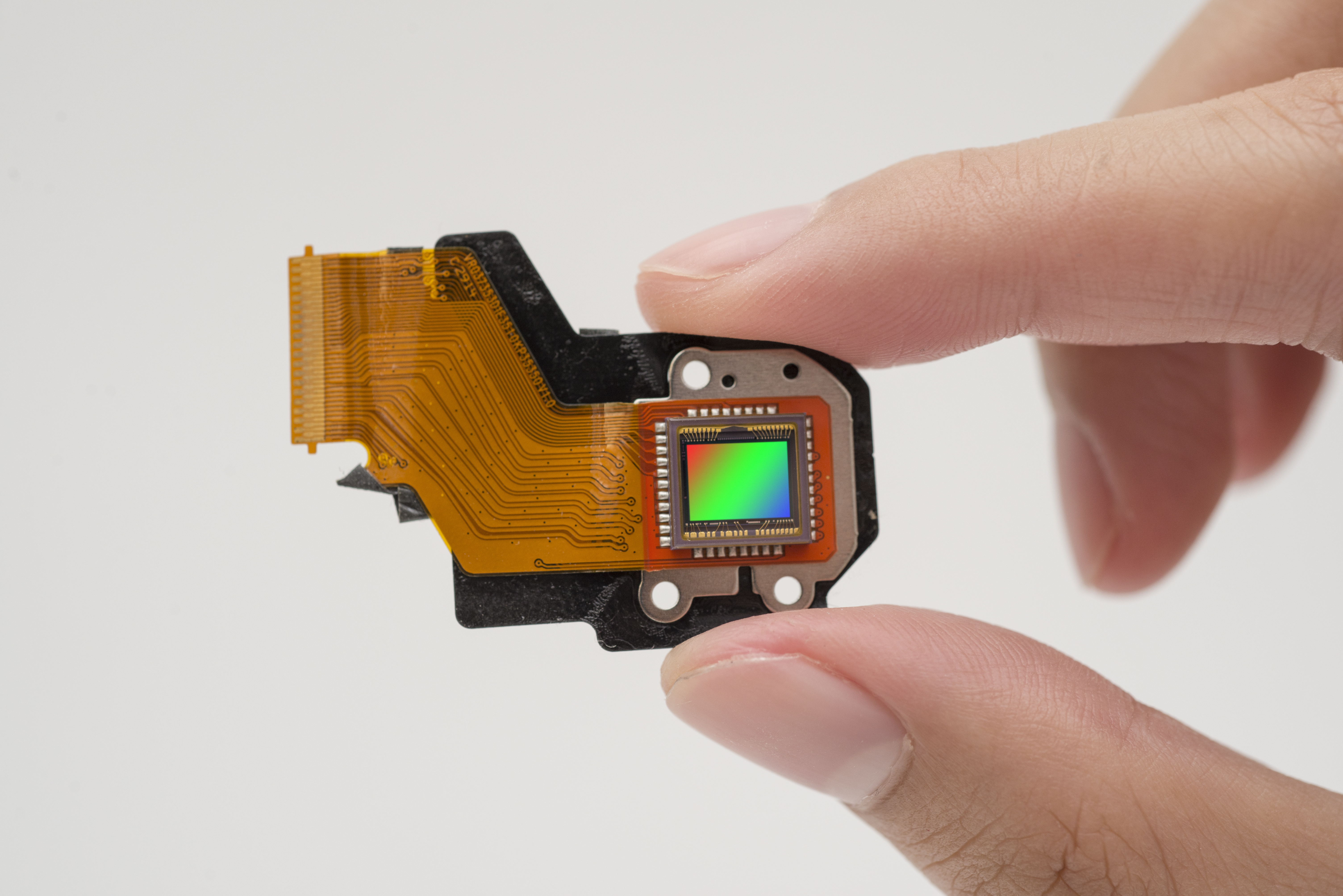
A classic use of photonics technology is the digital camera. The core component that allows digital cameras to function is a light sensor. This was originally a charge-coupled device (CCD) which consists of a patterned array of pixels to collect the light (photons) entering the camera lens. The sensitivity of the sensor depends on the efficient capture of light by each pixel. Since the array of pixels is itself a semiconductor device with circuitry between the pixels, it is not possible for the entire area of the sensor to be active pixels. One solution to this inefficiency is to fabricate millions of microlenses, one for each pixel, which collect the light that would otherwise be wasted hitting the circuitry or dielectric areas and focus it on the active center of the pixel.
There are many novel ways to pattern the hemispherical microlens arrays. They often take advantage of liquids' natural tendency to form perfectly round droplets due to surface tension. In this method, photoresist is patterned onto the device in a grid, with each cell corresponding to one microlens of the finished product. In a hot reflow process, the photoresist liquefies and forms nearly perfect hemispheres, each only a few microns in diameter. The resist will retain this shape as it cools and hardens. The round structure can then be transferred down to the layer below through an anisotropic plasma etch [1]. The etch need only be run as long as it takes to etch through the photoresist and does not need chemical selectivity. As long as the etch process is equivalent across the array of pixels, the pattern will be retained. For example, if the photoresist is 4 um thick, and the etch removes 4.5 um, the pattern will show up in the substrate. The substrate will have been etched 0.5 um at the centers of the features and close to 4 um at the edges between the microlens.
Etched Dicing Streets
One process that is unique to photonics chips is fiber attach. A photonic integrated circuit (PIC) generally requires one or more optical fibers attached for input and output of photons. Optical fibers are typically attached to the side of the chip to maintain the low profile of the device [2].
One challenge is that the side of a semiconductor device is usually rough and ragged. This is because the process of singulating a wafer into individual chips (dicing) is done with a grinding blade. For a good optical connection, the fiber needs to be attached to a very smooth surface.
This challenge can be met by a reactive ion etch (RIE). Before the mechanical dicing process, trenches can be etched into the top surface of the wafer where the blade will eventually dice. If this plasma etch is highly anisotropic, it can expose a very smooth facet where the fiber will eventually attach. The etch process need only be 100 um or so deep to make room for the fiber to connect to the edge of the chip. Since the silicon wafer is over 750 um thick, the 100 um trenches will not compromise the structural integrity of the wafer. The etched trench is also usually 50-100 um wider than the mechanical dicing blade that will be used for die singulation.
This will ensure that the dicing blade, when centered in the trench, will not damage the smooth etched sidewalls.
The material removed during the pre-dicing plasma etch process is silicon from the wafer substrate and silicon oxide from the top passivation layer, which surrounds the actual optical circuitry. For RIE etching of both of these compounds, a fluoride compound such as CF4 or SF6 is effective.
Optical Waveguide Fabrication
The actual light pathways (waveguides) of a photonic integrated chip are constructed of silicon pathways insulated from each other and the silicon substrate by silicon dioxide. Silicon can be used as a waveguide because it does not absorb infrared light. When the photons traveling in the silicon collide with the silicon and silicon dioxide junction, they are reflected forward along the waveguide, maintaining the light intensity. In this manner, the waveguides can carry and curve the light as needed to the various functional components of the circuit.
To fabricate the silicon waveguides, a SiO2 – Si – SiO2 sandwich is needed. This can be accomplished either by growing silicon on top of the native oxide on the silicon wafer or by implanting oxygen at some depth in a silicon wafer. Either way, a mask is then applied to cover the paths of the waveguide. A plasma etch process then removes the top silicon and the buried SiO2 everywhere except the paths covered by the mask. Thermal oxide can easily be grown to cover all exposed silicon. The result is a network of silicon completely buried and insulated by oxide. As the materials being removed are both silicon based, a fluoride compound is again an effective choice for this RIE etch process.
Conclusions
There are many more unique challenges to be faced in photonics fabrication. Here, we looked at how plasma etching is used to create sensors, to assist in the coupling of photonic integrated chips (PIC) with optical fibers, and to fabricate the optical circuitry of the PIC itself. In the first example, a non-selective etch that relies on ion bombardment is effective because the topography of the mask itself is what shapes the etch pattern in the substrate. In the second and third examples, a chemically selective RIE etch is preferred as the mask should not be etched at all.
While these are just a few of the ways that integration engineers have been able to use plasma etching to their advantage, there are other means available beyond just reactive ion etching. To learn more about potential etch solutions, download our eBook “Plasma Etching: Comparing PE, RIE, and ICP-RIE.”
 Citations
[1] Knieling, T., et al. “Microlens Array Production in a Microtechnological Dry Etch and Reflow Process for Display Applications.” Journal of the European Optical Society: Rapid Publications, vol. 7, 2012. Crossref, doi:10.2971/jeos.2012.12007.
[2] “Photonics: How Do You Attach Fiber to the Chip?” Breakfast Bytes - Cadence Blogs - Cadence Community, 20 Sept. 2020, community.cadence.com/cadence_blogs_8/b/breakfast-bytes/posts/photonics-how-do-you-attach-the-fiber-to-the-chip-120591603.


