It is not surprising that the scaling techniques used to enable Moore’s Law over the last several decades are being applied to similarly scale down the structures using macro-optics. As feature sizes of transistors have shrunk so that millions to billions of transistors fit on a chip, optical components have also been reduced in size. Many of these efforts are leading the way for advances in photonics. For example, chip-to-chip connections with relatively large fiber optics have evolved such that micron-sized chip-scale waveguides for making photonic based interconnects are now a possibility. Similarly, micro-lenses are opening up new applications that were once the domain of macro-lenses. This article introduces micro-lenses and how they are made using semiconductor processing techniques.
What are micro-lenses?
Micro-lenses are similar to optical components but are now in the millimeter to sub-micron regime. The lenses are like those found in macro sized world with the most common being the spherical or aspherical shape on a substrate. A second approach, a derivative of gradient-index (GRIN) technology used in fiber optic waveguides, uses changes in refractive index to focus the light. While forming a structure with two flat and parallel surfaces is attractive from a format perspective, they are more difficult to implement. A third well-known approach is creating structures referred to micro-Fresnel lenses which takes sections of a traditional lens and forms concentric circles with each section representing a part of the conventional lens. Those familiar with lighthouses would be familiar with Fresnel lenses used to project the lantern illumination. The three approaches are shown below, (a) traditional, (b) GRIN, and (c) Fresnel lens.

Another area of keen research interest is metamaterial lens or super lenses. These lenses combine materials, shapes, orientation, and sizes at the nanoscale to enable manipulation of light in ways not possible with conventional materials and shapes. For example, imaging below the diffraction limit resulting in new boundaries for resolution.
What are some of the applications for micro-lenses?
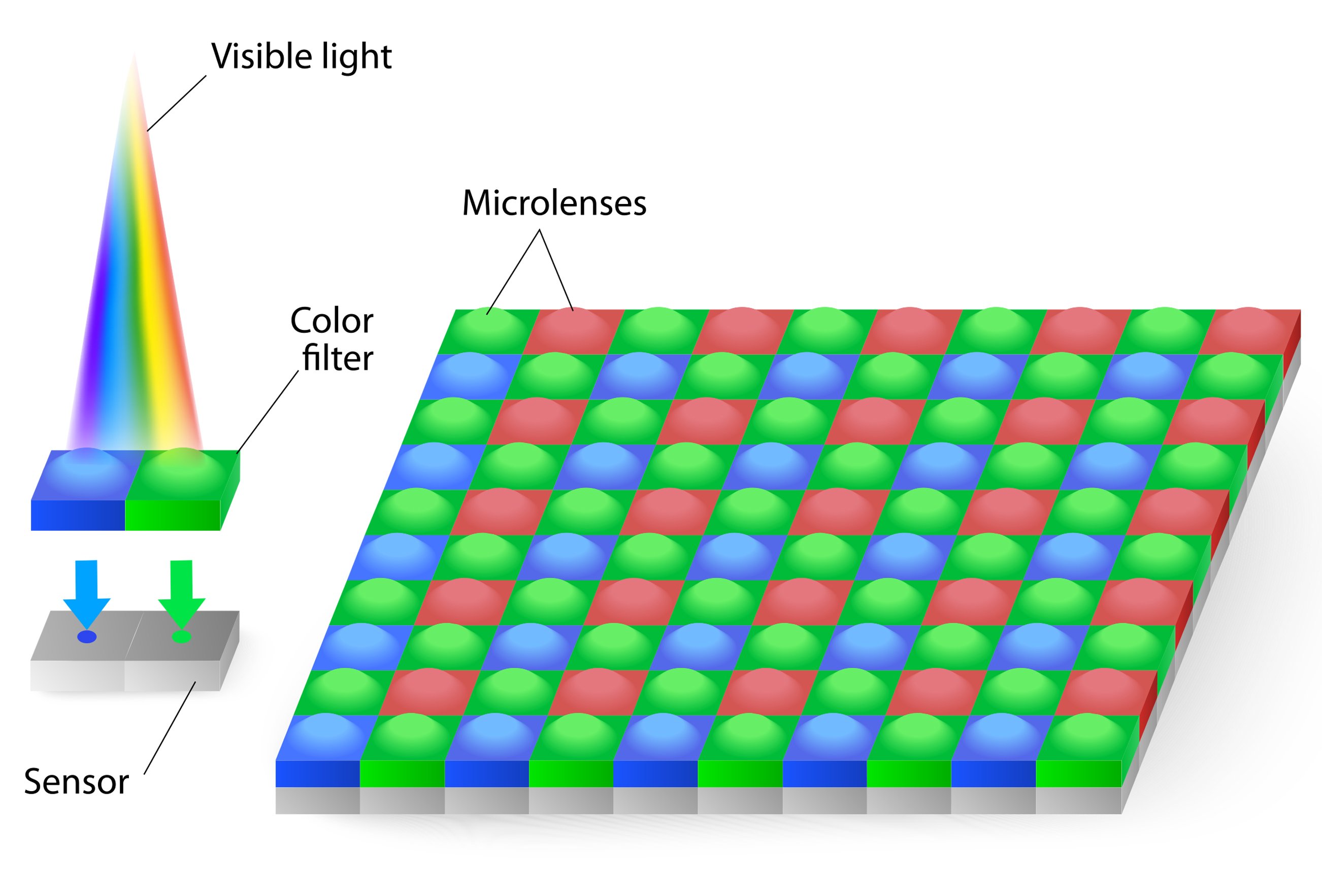
Micro-lenses can be used as individual components or in complex arrays. As an individual component, it can be used to enhance coupling performance between an optical fiber and a light source or detector. The form factor of arrays has enabled camera miniaturization that are found in phone cameras and displays. Mobile phone cameras are using arrays with many tens of millions of elements mated to similar numbers of CMOS sensor pixels. Other designs using stacked lens structures have resulted in camera technology for in-body medical imaging. It’s hard to believe, but cameras less than 1 mm in diameter are in use through advanced chip-scale packaging. Other areas of utilization include new approaches to photography that rely on image reconstruction and 3D imaging for virtual reality displays.
![]()
How are micro-lenses fabricated?
Micro-lenses with traditional lens shapes and Fresnel structures can be made by applying some of the fundamental processes in microelectronics, primarily photolithography and etching. (GRIN lenses are more complicated in their fabrication and will not be discussed within this article.)
The most common approach to fabricating micro-lenses involves transferring a structure made with photoresist into the lens material. Two requirements must be met to form the desired micro-lens: 1) the resist or polymer must be in the shape of interest and 2) the plasma etching process must have the appropriate etching selectivity between the photoresist or polymer and the lens material.
The approach for spherical or aspherical lenses is to form a structure in the photoresist and then with heating cause the photoresist to reflow. This allows surface tension to form the lens template. The second step uses plasma etching to transfer the shape into the lens material. Typically, the dry etch process is adjusted to provide a selectivity of 1:1 so the pattern fidelity is maintained. Modifying the selectivity to greater or smaller than 1:1 allows the fabrication of aspherical lenses. The same approach is used for Fresnel lens however the photoresist is usually patterned using a grayscale mask or by varying the dose during e-beam writing. Again, the pattern is transferred 1:1 between the resist and the lens material.
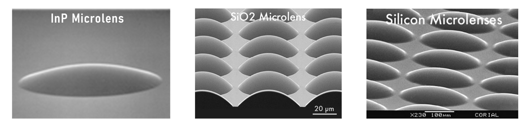
With a good understanding of the plasma etching process, micro-lenses can be made in a variety of materials to take advantage of their optical properties. Below are examples using Indium Phosphide (InP), Silicon Oxide (SiO2), and Silicon (Si).
Selectivity between the mask and the lens materials can be tuned by adjusting etching parameters. Substrate bias, plasma source power, temperature, pressure, and gas chemistry can all be used to influence the relative etching rates. While most dry etching processes strive for maximum selectivity, the replication of the mask profile with 1:1 selectivity usually requires lowering the selectivity. One of the challenges for production is maintaining the 1:1 selectivity while at the same time maximizing etching rates to achieve cost-of-ownership-driven throughput. Not only must the process produce the desired profile, but it must also deliver the smooth surfaces expected from optical components. For these reasons, the etching equipment is nearly always an inductively coupled plasma (ICP) reactor configuration. This configuration provides the requisite flexibility.
Summary
Microlenses are now an integral part of many important adopted applications that include mobile phone cameras, in-body medical imaging, microscopy, 3D imaging and projectors. Depending on the application, plasma etching can either produce micro-lenses that will be used in the application or produce the mandrill for molding or embossing large quantities. Plasma etching, with the variety of chemistry and processes possible, are able to produce micro-lenses in a wide range of materials that includes diamond, quartz, silicon, and compound semiconductors such as gallium arsenide (GaAs), indium phosphide (InP) and gallium phosphide (GaP). The capability to shape a variety of materials with different optical properties will continue to be important for micro-optics.