The promising technology to address the challenges of manufacturing next-gen micro devices
Conventional (i.e., continuous) etch processes no longer deliver the required level of control, as CDs approach the sub-10 nanometer scale.
To continue technology scaling in logic circuits and memory devices, atomic-level precision manufacturing is now required by chip makers and academics to ensure ultra-high etch selectivity, low damage, and control of features and surfaces at the nanometer scale.
ALE technology
Atomic Layer Etching (ALE) technology enables the controlled removal of material from a substrate, layer-by-layer, where the etch thickness is on the order of magnitude of a monolayer.
This technology is of growing interest for academic and industrial applications as an alternative to continuous etching, and as an essential counterpart to ALD.
Despite its apparent simplicity, it has taken several decades since the discovery of the ALE mechanism for the technology to gain broad acceptance and applicability.
Self-limited reaction is a key characteristic of atomic scale etching. Ideally with ALE, adsorption and desorption steps are self-limited at a maximum rate equivalent to 1 monolayer (ML) per cycle. The total amount of material removed is determined by the number of repeated cycles.
ALE process cycle
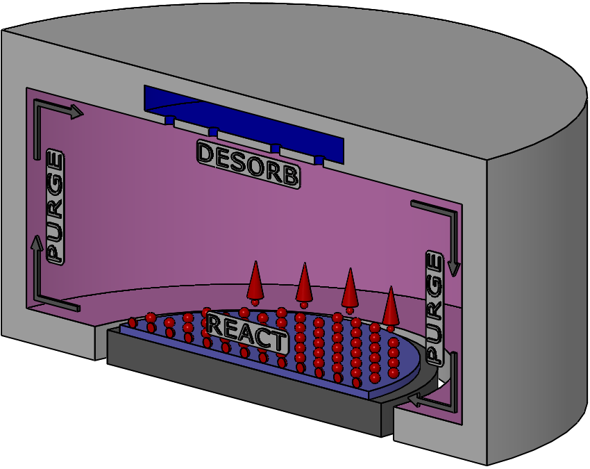
The ALE process sequence consists of repeated cycling of process conditions. Each cycle is typically comprised of 4 steps.
Adsorption
During step 1 of the cycle, reactive species are generated in the reactor (for example, upon plasma excitation), are adsorbed by, and react with material on the wafer. Due to the self-limiting process, and with the proper choice of reactants and process conditions, reaction takes place with only a thin layer of material, and the reaction by products are formed.
Purge
In process step 2, purging of the reactor is required to remove all traces of the reactant.
Desorption
The byproduct desorption process takes place during step 3, due to bombardment of the wafer surface by noble gas ions with a tightly controlled energy.
Purge
Byproducts are purged from the reactor during step 4.
ALE processes
Atomic Layer Etching is an appropriate technology for any application requiring:
- High etch selectivity
- Low etch damage
- Nanometer-scale control of film structure
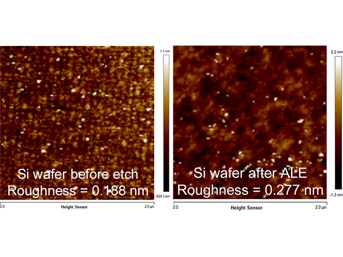
The process recipe parameters and reactants used in ALE enable etching with exceptional precision and selectivity to masks layers.
The materials suitable for ALE range from semiconductor and dielectric materials (Si, III-V, SiO2, Si3N4) to metals and 2D materials such as graphene, MoS2 etc.
Products
Corial 200 Series System for Atomic Layer Etching
Process control software for time-multiplexed processes
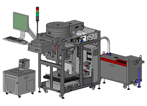
Corial 210IL
- Etch system with the capability to etch in ICP, RIE, ALE and DRIE mode in the same reactor
- High precision silicon ALE rate of 1.675 nm/min
- Reduced byproduct deposition on reactor walls for faster step switching
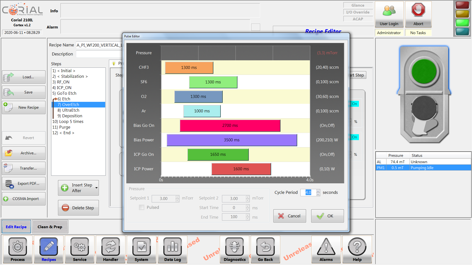
CORTEX™ Pulse
- Enables ALE process control on conventional ICP-RIE systems
- Advanced tuning of RF pulsing to control ion energy
- Independent and rapid pulsing of gases, down to 10 ms
- Real-time process adjustment
