Atomic Layer Processing (ALP)
Atomic Layer Processing designed for the next wave of Integrated Circuits?
Be selective, and choose CORIAL’s Atomic Layer Etching and Atomic Layer Deposition technologies (ALE/ALD)!

Fourth state of matter
Plasma is one of the four states of matter, along with solids, liquids, and gases. Plasma is an ionized gas consisting of equal numbers of positively-charged ions and negatively-charged free electrons. Thus, in plasma overall electrical neutrality is maintained.
Plasma is a common part of the world we live in. Along with nebula, interstellar space, and solar wind to mention a few, about 99% of the universe is made of naturally-occurring plasmas.
Plasmas are broadly used in technologies we interact with on a daily basis. Consider fluorescent lamps and neon signs – they are made of glass tubes filled with gas. When the lamp is turned on, the gas becomes ionized, electric current starts flowing through the tube, electric energy is dissipated, generating ions, electrons and excited molecules. This molecular excitation-relaxation process creates the characteristic plasma glow discharge inside the tube that illuminates the surrounding environment.
Plasma generation
The practical means to create plasma is to apply an electric field to a low-pressure gas.
Any free electron (created by a cosmic electron, for example) can be accelerated and gain enough energy to ionize a molecule by collision.
So, an electron/positive ion pair is created. The new free electron will continue the process and the plasma will be established by this chain reaction.
The move from thin films as we know them, to atomic layer processing
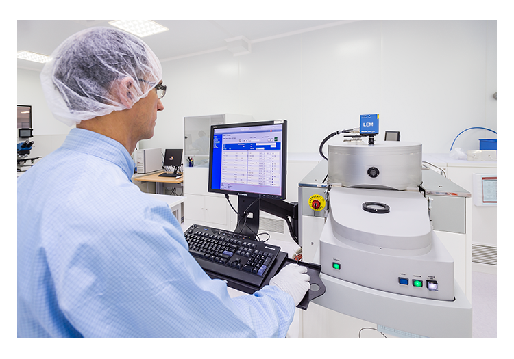
The scale-down of IC features, aggressive development of 2D materials, necessity of stringent control over deposited film thickness and etch depth, deposition conformality, and ultra-high process selectivity are each challenging on their own, and together they demand the transition to novel processing techniques.
Atomic scale processing, including Atomic Layer Etching and Atomic Layer Deposition, enables a high degree of process control and exceptional uniformity, on an atomic scale.
Atomic layer processing principles
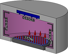
Both ALE and ALD technologies rely on surface reactions that limit deposition or etching.
Both processes are time-multiplexed (pulsed) with alternation of the process parameters (gas flow, applied power), all controlled by software.
Advantages of atomic layer processing
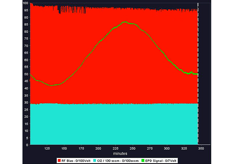
Ultra-high selectivity
Low damage
Highly accurate process control
Atomic layer processing technologies
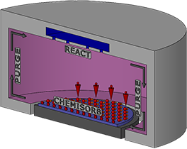
Atomic Layer Etching (ALE)
Etch technology enabling the controlled removal of material from a substrate, layer-by-layer.
Atomic Layer Deposition (ALD)
Technology to deposit films on a monolayer scale, which has become widely adopted in R&D and various industries.
