My Process Was Working, But Now It Doesn’t: Developing Robust Processes
Often a process worked or is working but then develops some irreproducibility or drift away from the target results. For one reason or another, the process has strayed from the process window that at one point provided the intended results. A robust process consistently delivers desired results despite the many variables vying to create instability and irreproducibility....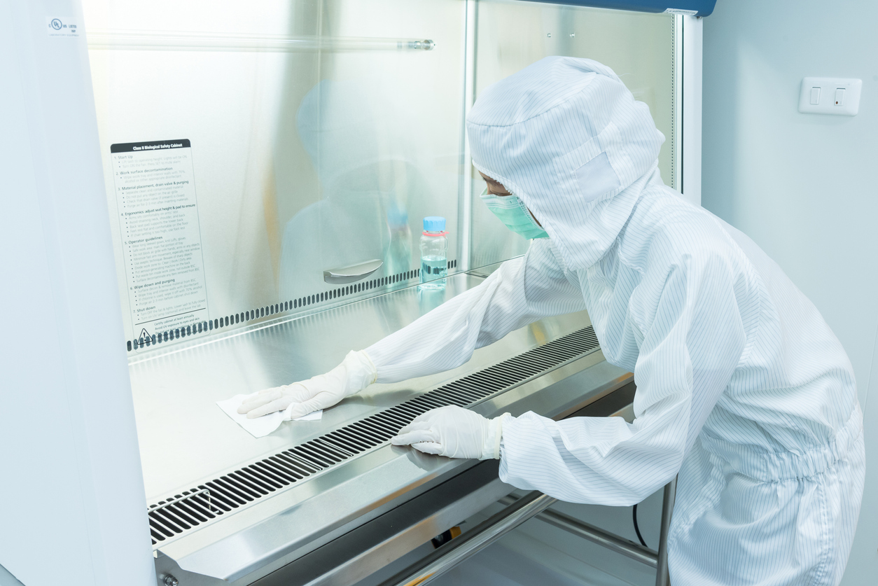
Chamber Cleaning: Keeping ICP Clean
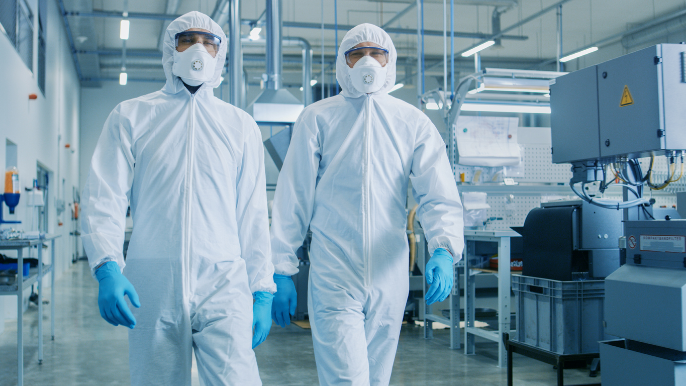
Plasma processing chambers are among the heaviest used types of systems in the manufacture of wafer-level electronics. Whether it be for discrete device research or more complex integrated circuits, plasma processing plays a critical role. For this reason, it is important to understand how to keep it at optimum operating performance....
The Versatility of Plasma: Interview with Dr. Steven Shannon
Dr. Steven Shannon is a Professor of Nuclear Engineering and the Director of the Nuclear Engineering Graduate Program. He works in the area of industrial applications of plasma discharges and his research focuses on enhancing current plasma applications and developing new plasma applications for next-generation material and device fabrication....
Diamonds and Beyond 5G: A Conversation with Prof. Srabanti Chowdhury
Srabanti Chowdhury, PhD., is an Associate Professor of Electrical Engineering at Stanford University. She received the DARPA Young Faculty Award, NSF CAREER and AFOSR Young Investigator Program (YIP) in 2015. In 2016, she received the Young Scientist award at the International Symposium on Compound Semiconductors (ISCS). We interviewed Prof. Chowdhury to discuss her research on wide bandgap materials and energy efficient device engineering....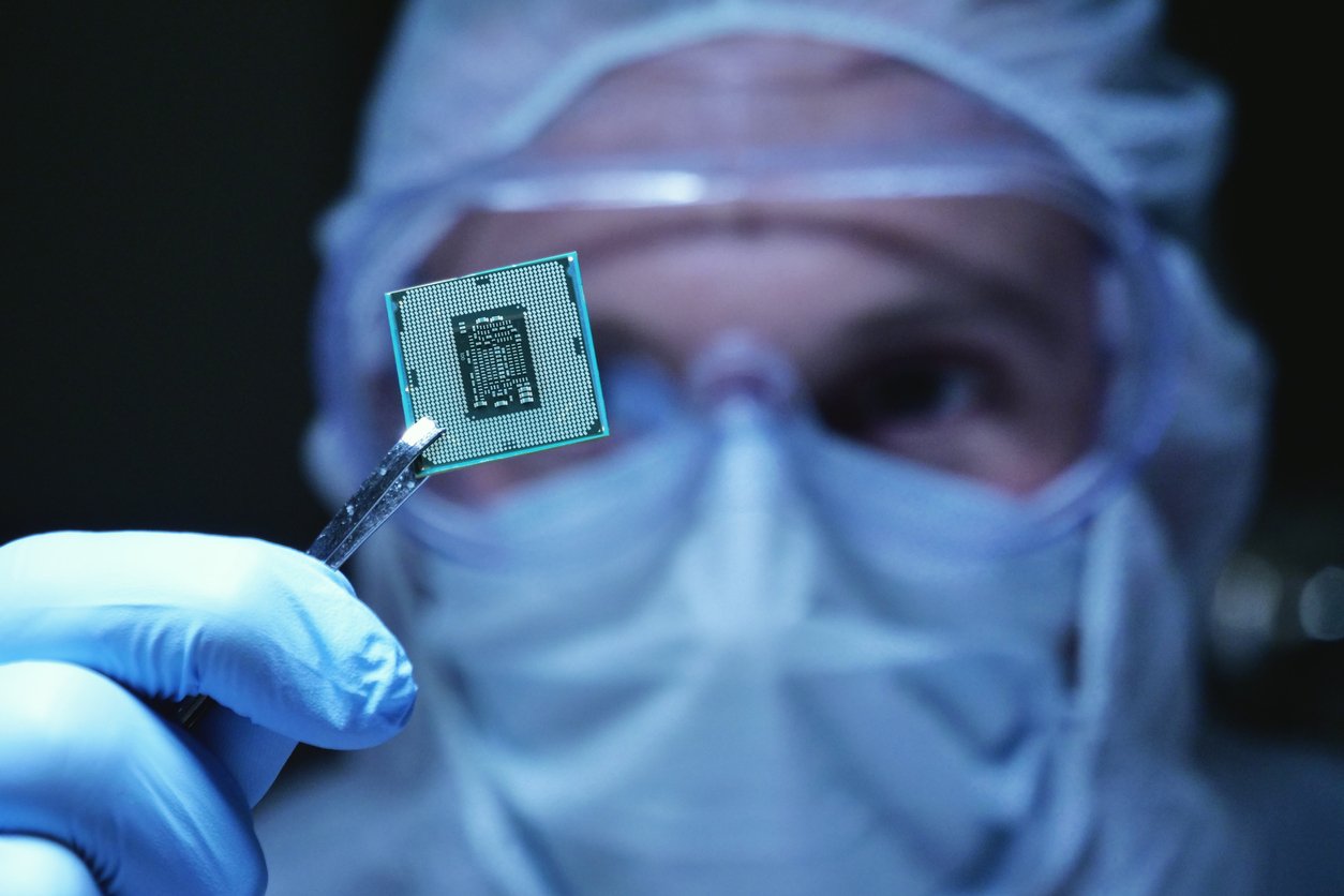
Introduction to Failure Analysis
Today’s electronic chips are a complex composition of devices intricately connected to form a highly-functioning unit. The devices or integrated circuits include simple resistors, capacitors, inductors, and diodes coupled with the more complicated transistors. To give an idea of the complexity, the chips running today’s advanced processors contain billions of transistors at a density of nearly 300 million transistors per square millimeter. At these densities, the heat density starts to approach that of the sun. The performance of integrated circuits at an ever-shrinking scale is truly amazing....