Wafer Singulation FAQ
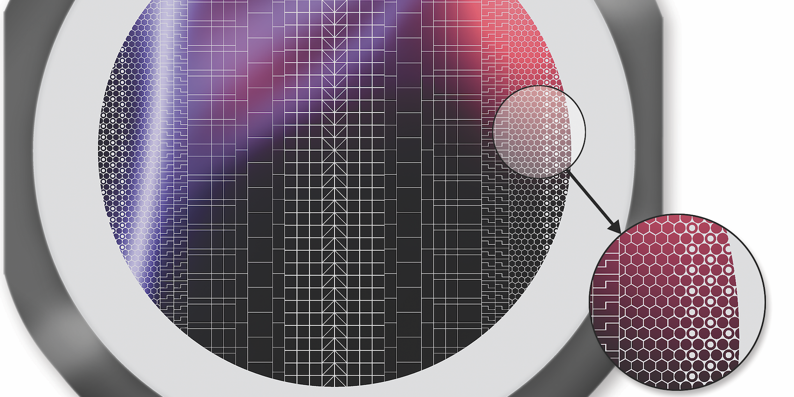
What is wafer singulation? Wafer singulation is the process of cutting or dicing a finished wafer into individual chips. Integrated circuits are typically built on a thin, round wafer of silicon used as the substrate for wafer processing for semiconductor manufacturing. The slices of silicon can be up to 18 inches and contain hundreds to thousands of individual die. The dicing process, or singulation process, is where a wafer dicing technique is used to cut each die with a diamond blade, laser, or plasma into individual chips that can be later mounted and assembled in advanced packaging....
CORIAL's Top 5 Blog Posts of 2021
As a Plasma-Therm company and leader in the plasma-processing and advanced-packaging industry, our finger is on the pulse of the semiconductor and nanotechnology markets. Over the past year, we’ve shared educational and informative information regarding plasma-etching, deposition, product highlights, and other relevant tech news and updates....
How to Resolve Vacuum Chamber Issues
Few issues haunt plasma processing quite like vacuum chamber problems. Plasma etching and plasma deposition tools require vacuum to be able to maintain the plasma and control the gas composition in the process. Other non-plasma deposition processes such as physical vapor deposition require a vacuum for the deposition species to reach the substrate without colliding with gas in the chamber. Creating and maintaining the vacuum can be complicated but is crucial to the success of the process....
3 Specialized Etch Processes for Photonics Fabrication
There are typical etch processes that are used in nearly every process flow, but there are also specialized etch processes that are specific to unique aspects of the application. Photonics manufacturing is no exception. Whether fabricating image sensors or photonic circuits, dry etch processes will be key to creating features with excellent optical properties....
How to Minimize Downtime for Etch and Deposition Equipment
Semiconductor plasma etch and deposition equipment has drastically different usage profiles when used in industry as compared to its use in research and academia. While the physics governs both applications, their end uses are different, and thus require different considerations for optimization....