What is wafer singulation?
Wafer singulation is the process of cutting or dicing a finished wafer into individual chips. Integrated circuits are typically built on a thin, round wafer of silicon used as the substrate for wafer processing for semiconductor manufacturing. The slices of silicon can be up to 18 inches and contain hundreds to thousands of individual die. The dicing process, or singulation process, is where a wafer dicing technique is used to cut each die with a diamond blade, laser, or plasma into individual chips that can be later mounted and assembled in advanced packaging.
Having a good die singulation process is essential for yield and quality, and the technique chosen is based on parameters such as die strength and wafer thickness. The value of the wafer increases considerably by the end of the manufacturing process. During the last part of manufacturing, wafer singulation is an expensive time to cause damage. Some of the die side damage that can occur during the singulation process is topside, backside, and sidewall chipping, reducing first-pass yield and usable die count.
There is a need to strike a balance between throughput and damage to the wafer such as backside chipping. Slowing the processing speed will increase cycle time and decrease throughput but can preserve the side of the wafer. However, process changes such as increasing the RPM of the spinning blade for mechanical dicing can also sacrifice good yield caused by die damage.
What is the wafer singulation process?
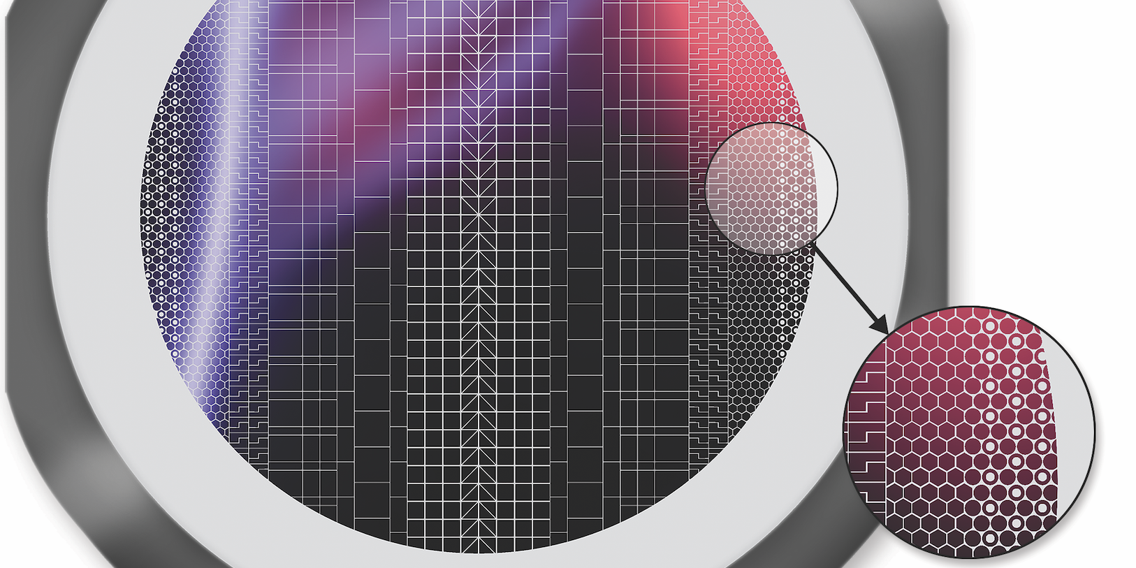
The wafer singulation process consists of several steps intended to separate each die by cutting down the middle of the street or scribe lane created between chips. There are four types of wafer singulation processes that will be discussed. There is a blade process that uses mechanical grinding. The two laser scribing processes are ablation and stealth dicing which uses melting and evaporation or thermal and mechanical processes respectively. The last is plasma dicing which uses chemical etching. Die strength is a critical parameter for thin and ultra-thin dies. Plasma dicing has the potential to achieve much higher die strengths by reduced notching when compared to the other dicing approaches mentioned.
There are many important factors to consider when optimizing the singulation technologies. For mechanical dicing, the main factors to consider are:
Water flow rate: Water flows on the blade and wafer for cooling and debris removal. The flow of water is important for minimizing wafer damage and eliminating post sawing silicon dust.
Blade height: Distance from the blade to the chuck table. If the blade is lowered to the distance of the chuck table, it can damage the blade if it comes in contact with the chuck table. The goal is to complete the cut through the silicon substrate and the backside wafer tape without hitting the chuck and with minimum cutting damage to the die.
Dicing method: Important parameters when considering a dicing method are between the single or double spindle dicing machines. Consider manufacturing needs such as four types of cuts: Single cut, duel cut, duel pass, and step cut. Step cuts with thick material and fast blade RPM can be used to minimize backside damage due to cut stress.
Blade RPM: Rotation per minute of the stationary blade
Feed speed: Velocity of the chuck that moves the wafer back and forth to the blade
Although mechanical blade dicing was the workhorse of die separation, new challenges have appeared with the need for low-k or copper structures, wafer thinning, die edge quality, narrow dicing streets, and complex backend processes that may require consideration of a different technique.
Specifically, the challenges of mechanical dicing are solved by using plasma dicing.
What is plasma dicing?
Plasma dicing is a cutting technique that uses plasma etching as a means to separate the individual chips. The main types of non-blade dicing include ablation, stealth, and plasma. These alternatives provide the advantage of minimizing residual stress to the wafer and chipping due to the cutting process. Ablation is the process of melting and evaporating material to be removed with a laser. It is a good process for low-K devices as it reduces damage compared to mechanical sawing. It does require water cooling and contact with the wafer surface.
The stealth process also uses a laser for cutting but employs internal adsorption instead. It is a dry process that produces minimum damage. The stealth process involves focusing the laser beam on a small area below the wafer surface. The laser modifies the area within the scribe line in which it is focused creating a fragile area easier to break under mechanical stress. The wafer is then pulled apart by crack propagation separating the individual chips. The laser and blade process can be used together for singulation. The laser can provide a path to remove the top layers such as low-k and metal layers leaving the blade to finish cutting the silicon substrate and wafer tape below.
Plasma dicing is a chemical etching process using plasma to etch the desired material in the scribe lanes. Just like in the etching process used for the semiconductor build, the finished wafer gets a photo litho layer spun and baked onto the surface where the scribe lines are exposed for etching. The fluorine-rich plasma etches troughs the streets between chips using deep reactive ion etching (DRIE) to complete the valleys. The masking layer is removed, and the wafer is cleaned post-etch/photo processing. Isotropic and passivation etching can be performed in the same chamber to yield many desired etch shapes and scalloped sidewalls.
The advantage to plasma dicing is its ability to etch the entire wafer at once instead of blades or lasers which move across the wafer in several repeated passes. It can also etch areas that are not rectangular unlike a blade or ablation processes. It adds additional processing steps such as photolithography and cleaning but eliminates both mechanical and thermal stress caused by the other types of dicing.
What is the wafer mounting process?
The wafer mounting process occurs before the singulation process to stick the wafer to the wafer ring using tape. If the dicing technique requires the wafer to be held in position, then some type of tape is needed on the backside of the wafer. Typically, the objective is to stick the wafer to the wafer ring using mounting tape. The wafer is usually a round slice of silicon that contains semiconductor chips. The wafers have four important characteristics for processing: wafer size, wafer thickness, die size, and saw street width.
The mounted wafer becomes the carrier for the sawing process. During the sawing process, the cut goes through the wafer and partly into the tape. Then, the tape is removed, leaving the individual chips for the rest of the backend process.
How are silicon wafers cut?
The silicon wafers are cut during the singulation process using a dicing technique. Currently, there are three main types of wafer cutting on the market including mechanical dicing, laser dicing, and plasma dicing. Mechanical dicing uses a blade that physically saws the wafer into individual dice. Laser techniques employ a laser beam to slice the streets between individual dice. Plasma dicing uses a chemical reaction involving plasma which etches the areas not protected by a mask layer. Mechanical dicing tends to produce higher chipping during processing, a larger sawing kerf, and more quality issues due to blade wear. The laser technique leaves burn marks beside the kerf and has significantly higher machine costs. Plasma dicing is used for more critical devices that demand exact cutting precision and lower chipping events.
What is a wafer kerf?
The wafer kerf is the width of material removed during the cutting process. The kerf is an area in a silicon wafer that is used to separate individual chips at the end of wafer processing. This area also contains features that assist in the manufacturing process but are not present in a final product. The overall design of scribe line features can be drastically different from the die layout. The scribe line, with intermittent regions of low and high pattern density, is naturally more prone to overpolishing, an issue that is exacerbated by thickness variation at the wafer edge. This design can result in yield loss for the prime die. When evaluating dicing technologies, the kerf is an important variable to consider.
What is wafer scribing?
Wafer scribing is a process in which the wafer or substrate is partially cut through the scribe lane, and then a breaking process is used for the final singulation of the chips. To break the wafer, a scribe line must be created on the wafer surface. This line creates stress so that the wafer breaks along the line after a force is applied. This wafer-level scribe and break technique enable narrow scribe lanes while maintaining a low heat affected zone (HAZ). It also has a narrow kerf width meaning more usable die per wafer while still maintaining maximum process speeds for high production throughput. Scribe and break-die separation is an alternative to saw dicing. The features of scribe and break die separation is especially beneficial with thin silicon wafers, delicate III-V materials, and hard materials.


