What is the throughput of a plasma processing system? When buying a system, it’s important to know whether the level of output is suitable to fulfill the user’s capacity needs. For example, some customers are interested in how many wafers per hour can be run while others are asking how many chambers are needed to satisfy a quota of devices (units) in a month. Multiple factors go into calculating throughput.
Automation Choices
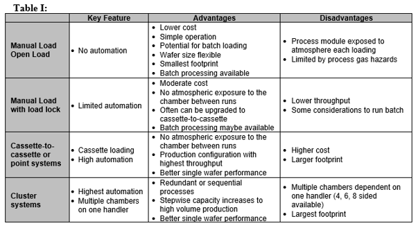
As the need for high throughput increases, the level of automation required increases as well. In R&D environments, throughput is usually not as much of a concern. They tend to favor manual open load or manual load lock systems. There are still some production models that strongly rely on manual operations. These systems are usually operated in a batch mode where many wafers can be processed simultaneous.
Table 1 shows some of the key features, advantages and disadvantages of the different handling options.
Factors Contributing to Throughput
Throughput can measured in many ways. For simplicity, assume a fully automated system where the operator loads and unloads a cassette and the system does the rest. The following factors will apply:
- Raw throughput: Refers only to the handling throughput without any processes. Raw throughput is a function of robot handling speed, and it can be on the order of 30 wafers per hour. There are some variation depending on the alignment requirements that can happen inside the transfer module.
- Process Time: There are processes such as those for backside vias and MEMS devices that can easily take nearly an hour per wafer. Other processes only take a minute or so. For these shorter processes, the automation is not the limiting factor.
- Process Throughput: This includes the handling time and overhead associated with running a wafer: Waiting for a loadlock pumpdown, moving the wafer into the process module (including alignment), clamping the wafer, waiting for gas flow and pressure stabilization, and then the times to de-clamp, pump out the chamber, and get the wafer back to the cassette and vent.
- Chamber Cleans: Some processes need a plasma clean every so many RF hours or wafers. Other processes require the chamber to opened periodically and manually cleaned. (one example might be cleaning windows used for endpoint). It can take hours to pump down a chamber after exposure to atmosphere to remove water vapor and residual gases such as oxygen. Both the mean time to clean (MTTC) a chamber and the cleaning frequency or mean time between clean (MTBC) are important variables. Each process has a characteristic clean cycle that can be estimated but only be known when it is determined with production data.
- Runs: Once the chamber is clean or “green” (referring to ready lights on the system) and ready to go, there might have to be a conditioning run to put the chamber condition into a known state. There may also be a qualification run to make sure it is ready to run product wafer.
- Uptime: Usually, this is typically between 85% and 95% but it depends on the tool and the process. One must also differentiate between downtime due to scheduled and unscheduled maintenance.
So, when asking for “average” throughput, it is not easy to answer without knowing what factors to include. The details matter. Things get really complicated when there are multiple chambers on a single handler. Other complications arise when there are cooling stations involved. Depending on the process times, scheduling the robot becomes complex.
Batch Processing
Batch processing often is considered when the wafer or substrates are small compared to the 200 mm and 300 formats found in mainstream silicon production. There are many applications that rely on substrates that for a variety of reasons are limited to 150 mm and smaller. A few examples are indium phosphide for optotelecommuncations, lithium niobate, and lithium tantalite wafers for RF filters. It is only recently that sapphire substrates for gallium nitride LEDS and gallium arsenide for RF power amplifiers have transitioned to 150mm wafers
When white LED use began its rapid grown, the sapphire substrates were at 50 mm. To reduce production costs and avoid processing one wafer at a time, the production model looked at operators loading pallets of wafers that would sometime exceed 40 wafers per process run. The challenge becomes how to achieve the requisite performance (primarily uniformity) with such large batches. Systems grew in size and the economics are such that these systems are still in production today but with 100 mm and 150 mm wafers. Due to limitations in chamber sizes, most high volume production is done with process modules designed to deliver high performance with single wafer loading.
Finding throughput depends on clearly outlining the assumptions that will be used in the calculation. The result of this calculation is used as one of the inputs when determining the cost-of-ownership of a system. In another blog we will discuss cost-of ownership that considers how one calculates that important parameter.