Deposition, a process used to deposit thin layers of material (or film) onto a substrate, is a commonplace practice in industries such as semiconductors and nanotechnology. Thin film deposition can be achieved with a variety of technologies that can provide films ranging from insulators to semiconductors to metals. The films can serve roles equally diverse that range from interlayer dielectrics to interconnects.
Considering a Deposition System? Some Things to Think About
In this blog the discussion will focus primarily on films deposited with chemical vapor deposition (CVD) technologies such as plasma enhanced CVD (PECVD) and a subset known as high density plasma CVD (HDPCVD). However, the guidance herein applies to other deposition technologies such as atomic layer deposition (ALD) and ion beam deposition (IBD).
Like other fabrication processes, deposition processes requires very specific film characteristics to obtain needed performance. While industry often relies on well-defined and well-understood materials, R&D is pushing the capabilities with advanced materials will have impact on future devices and structures.
This short work is intended to provide the reader with a brief overview of some factors that impact deposition performance. Each of these factors needs to be weighed carefully, considered thoroughly, and fully understood to ensure compatibility across your system.
Understanding Deposition
Typically deposition is divided into two large categories: physical vapor deposition (PVD) and CVD. While PVD uses heat or sputtering to physically transfer materials to vacuum and then to the substrate, CVD uses gases to provide the precursors for the film to be grown. PVD films are usually deposited with the substrate at relatively low temperatures. The CVD usually requires the substrate to be at an elevated temperature. Plasma can assist the process and allow a lower substrate temperature. See the whitepaper comparison between low pressure CVD (LPCVD, HDPCVD and PECVD for more insight on these technologies. There can be overlap between the two technologies as in the case of reactive deposition where the precursor is provided by PVD and reacts with a gas to form a new material. One example is aluminum sputtered with an ion beam that reacts with oxygen to form aluminum oxide.
As with etching, deposition processes are also a complex and require a good deal of experience and knowledge to be able to tailor film properties to specific applications. The purpose of this article is to explore film characteristics and by better understanding film characteristics, have better insight into depositing them.
Let's look at some of the factors to consider when using or acquiring deposition equipment.
-
1. Deposition Rate
Deposition rate, simply a measure of how fast the film is grown, typically uses units of thickness divided by time (e.g. A/s, nm/min, um/hour). As with etching, it is important to choose a technology that provides a deposition rate commensurate with the applications. For example, one would utilize a relatively slow deposition rate for thin films (just like in etching thin films where one uses a relatively slow etch rate) and correspondingly, a fast deposition rate for thick films. The idea is to maintain control and balance the need for speed and the need for precise control of the film thickness. But of course there are always tradeoffs between film properties and process conditions. Faster rate processes often use higher power, temperatures, or gas flows that affect or limit other film characteristics such as uniformity, stress, or density.
Deposition rates may range from as low as a few tens of A/min up to a 10,000 A/min. There are techniques to monitor the film thickness growth in real time a variety of methods such quartz crystal monitoring and optical interference.
-
3. Uniformity
Deposition uniformity is a measure of film consistency in across a substrate. Usually it refers to film thickness but it can also refer to other film properties such as index of refraction. The collected data across a wafer is usually averaged with a standard deviation representing the deviation from the average in terms of one, two or three sigma. An alternative approach is to use the formula of ((maximum value –minimum value)/2 x average values). One must remember to identify a zone where the metrology should be excluded due to clamping or other edge effects.
It is useful to have a good understanding of the application to avoid over or under specifying uniformity. Films that play a direct role in the device operation such as a gate oxide or a capacitor thickness, are much more likely to need a tighter uniformity specification than films that do not (e.g. an encapsulation layer). Uniformity not only plays a role in device performance but from a manufacturing perspective it is important to realize that other steps may be impacted by poor uniformity. A film with poor uniformity will impact etch steps by affecting the time it takes to etch the thinnest portion of the film versus the thickest.
3. Flexibility
Flexibility, the range of capabilities a system has, is may a significant factor in making a decision on which type of deposition system to acquire. This is truer for R&D environments rather than industrial applications where specific solutions are often preferred. Understanding the materials that can be deposited, substrate sizes, temperature ranges, ion flux, deposition rates, frequencies, endpoint, and pressure operating regime are just some of the considerations. Flexibility is also a system quality that allows planning for the future. In R&D priorities changes and it is useful to have a system that can handle those changes. Layered on top of these consideration is budget. Depending on the type of technology options, systems can vary in price significantly.
-
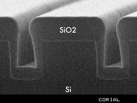
4. Step Coverage
How a deposition process to covers the substrate topography is described as step coverage or fill capability. Step coverage is measured as the ratio of a deposited film along the features sidewalls or bottom to the deposited thickness in the open area without features. For example, a feature that has 0.1 um of deposited film along the sidewall of a trench and has 0.15 um of film in the open area, has a step coverage of 67%. The deposition mechanism (e.g. CVD vs. PVD vs. IBD vs. ALD) plays an important role in determining the step coverage and fill. In some deposition technologies such as evaporative deposition, the vacuum pressure is very low and the depositing materials arrives in a line-of-sight approach from the deposition source. In other technologies, the pressure is significantly higher and because of gas phase collisions the material arrives at the surface from all angles. Temperature, feature profile and aspect ratio all affect the amount of step coverage and ability to fill a feature.
-
5. Film Characteristics
A film’s properties depend on the application. We can roughly group the application requirements into categories such as photonic, optical, electronic, mechanical, or chemical and often films must satisfy requirements in more than one category. For example, hydrophobic films such those used on the Apple products to protect the surfaces from moisture damage (chemical requirement) also need to be transparent (optical). So the first step to depositing the appropriate film is understanding the application and how the film properties affect the final performance in the application. It is not necessary to specify all film properties for all applications.
Below is a list that provides a starting point of film properties to consider.
|
· Wet etch rate · Pinholes · Adhesion · Density · Refractive index · Dielectric constant |
· Hermeticity · Hydrophobicity · Conductivity · H concentration · Breakdown voltage · Morphology |
Some films are only meant to be used as a hardmask for a future etching step. In this case, the electrical and optical properties of the film are of little importance. However, a film that would be used as a waveguide would need to have carefully controlled optical properties such as refractive index.
-
6. Process Temperature
Film properties are strongly influenced by process temperature. However the application can impose limits on the temperature that can be used. For example, recent interest in flexible electronics which often utilize polymeric substrates, have are limited by the melting point or reflow temperature of those polymers. Some compound semiconductors such as GaAs are limited by ohmic contacts which degrade at higher temperatures. The various deposition technologies operate best in limited temperature ranges. A guide with some typical temperature range values is provided in the following table:
|
Deposition Technology |
Typical Substrate Temperature Operating Regime |
|
Ion Beam Deposition (IBD) |
<100 °C |
|
Atomic Layer Deposition (ALD) |
<200 °C |
|
E-beam evaporation (PVD) |
<100 °C |
|
Sputter deposition (PVD) |
<200 °C |
|
HDPCVD |
<150 °C |
|
PECVD |
200 – 400 °C |
|
LPCVD |
600 – 900 °C |
-
7. Process Robustness (Productivity)
Productivity addresses system performance aspects rather than the films themselves. This is where one considers issues such as reliability, stability, and maintenance. Reliability is a measured by productive uptime while stability is measured by the system’s run-to-run reproducibility.
Since deposition systems are adding material to the closed system, over time there can be an increase in particle counts. The sensitivity of the application to particles as one part of the equation in determining when cleans should be done. This leads to the maintainability of a system where it is desirable to have as lengthy as possible mean-time-between-cleaning (MTBC) and as short as time as possible for the mean-time-to-clean (MTTC). Cleaning for deposition systems may be as simple as a plasma cleans as found in PECVD systems or more complicated where shields need ex situ cleaning as in sputter deposition systems. A fast, efficient clean cycle with a fast post-clean requalification is clearly a plus.
-
8. Damage
As features continually get smaller, they generally become more sensitive to process damage. Each deposition technology has the potential to induce damage to the material being deposited upon. However, damage is not a simple topic. Understanding and measuring damage can be quite challenging as the mechanisms of damage may be complex and the damage itself, very subtle. Damage may be from ion bombardment, contamination, or ultraviolet radiation and there may be multiple sources of damage at once. Often the requirement is “no damage” but there is little thought to how damage can be observed without the lengthy task of making a completed device and not introducing other artifacts. It's important to understand the constraints of your equipment and your materials.
Want to Learn More?
Check out our free PDF "How to Choose the Right Plasma Etching and Deposition Partner" to learn more about the factors that determine performance across deposition and etching.