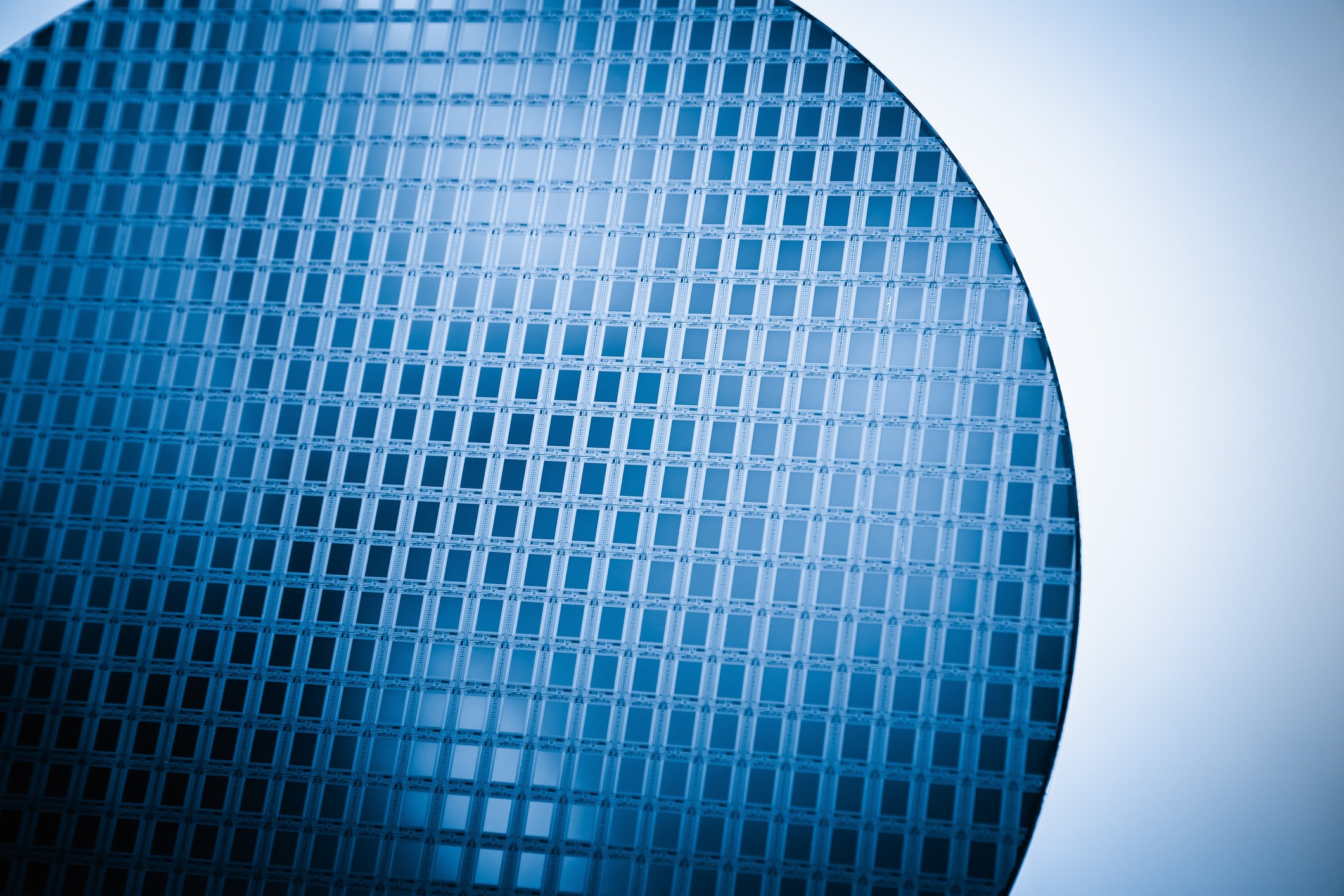
Introduction to HDPCVD
No doubt technology has experienced incredible acceleration since the development of the first transistors nearly 75 years ago. Key to that acceleration is the semiconductor industry and its fabrication methods that enabled low cost production of devices that now fuel nearly all aspects of our lives with ubiquitous advances in communication, healthcare, defense, transportation, and computation. Despite concern that the fundamental technology drivers of reduced size and cost are being challenged at the leading edge, there is certainly efforts that continue to ensure rapid progress
Those efforts include research and development of new materials and new structures that will deliver the requisite speed, power efficiency, new function or simply provide a new format. Whether it be new THz devices, IOT sensors, GaN HEMTs, MRAM memory, metamaterials, or flexible electronics there will be a need for new fabrication approaches.
One area of substantial interest is the search for lower temperature processing and within this search significant attention is being directed at thin film deposition. The thermal budget when working with many of these new materials is being reduced and the temperature must be lowered while maintaining much of the same performance as obtained at higher temperatures. For many thin film deposition processes the temperatures have decreased from furnaces running at over 1000°C to plasma enhanced chemical vapor deposition (PECVD) processes with temperatures in the 250 to 350°C range.
To push this temperature boundary even lower, many are looking at high density plasma chemical vapor deposition (HDPCVD). With HDPCVD the < 200°C temperature deposition range is opened up along with some new capabilities.
What is HDPCVD?
HDPCVD uses an inductively coupled plasma to generate a significantly higher plasma density than that derived from more conventional parallel plate PECVD configurations. In addition, HDPCVD includes the capability to bias the substrate, a feature usually absent from PECVD. This combination encourages denser films at lower temperatures than deposited with PECVD and adds capability to assist in planarizing patterned surfaces and fill higher aspect features such as trenches and holes without creating voids.
Ready to Learn More About HDPCVD Equipment?
Choosing between CVD systems isn't always easy. Each system having unique hardware, deposition capabilities, operating regimes, and functions makes them preferred for specific circumstances. To learn more about HDPCVD equipment, including the hardware details, technical details, and comparison tables, download our whitepaper "Chemical Vapor Deposition Comparison: LPCVD vs. PECVD vs. HDPCVD."


