Our Process Team has recently developed a process recipe for deep etch of silicon-based MEMS structures on SoI wafers.

Process recipe
This new recipe confirms the capability of our Corial 210IL ICP-RIE etch tool to achieve deep Si etching and at the same time to address all the usual applications of Corial ICP-RIE machines after quick (30 mins) conversion.
CORIAL Bosch-like process has 3 steps
- step 1 – polymer deposition by C4F8 plasma
- step 2 – polymer etching by SF6 plasma
- step 3 – Silicon etching with 20W of RF power, which was used to increase the silicon etching rate.
To alternate between each step, COSMA pulse software is required for pulsing consecutively C4F8 gas flow, SF6 gas flow, LF and RF power.
Corail 210IL ICP-RIE tool with DRIE configuration
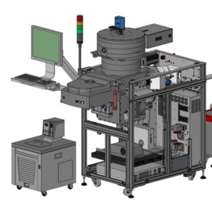
- High power (2 KW) ICP source producing uniform high density plasma,
- High power (1 KW) RF source to ensure high silicon etch rates,
- ICP source with the hot quartz liner allowing to diminish loss of reactive species,
- Very high conductance pumping system for operation at high gas flow rates,
- Helium pressure to ensure the thermal transfer between the cathode, the substrate holder and the substrates,
- Aluminum brace between ICP source and vacuum vessel to balance the ion and reactive species fluxes in order to enable Bosch-like processes,
- COSMA Pulse software enabling time-multiplexed processing,
- Capability to process a wide range of materials including silicon, oxides, nitrides, polymers, metals, III-V & II-VI compound semiconductors, and hard materials after quick hardware conversion.
Process performances for application #1
- 60 µm etch depth demo for a process requiring to stop on an SiO2 layer buried at 60 µm below the substrate surface,
- Open Si area is 10%, the rest surface was covered by Kapton.
- 5 µm feature size
- Etch rate 1.4 µm/min
- selectivity vs. SiO2 110
- Profile > 90°
- AR 1:17
- Uniformity over 4’’ wafer is 4% with exclusion zone of 10 mm
Process performances for application #2
- 200 µm etch depth demo for a TSV process,
- Open Si area is 10%, the rest surface was covered by Kapton.
- 5 µm feature size
- Etch rate 0.91 µm/min
- AR 1:33
- Selectivity vs. SiO2 >70
- Profile Anisotropic
- Uniformity over 4’’ wafer is 4% with exclusion zone of 10 mm


